FPGA Design
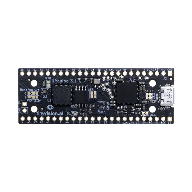
For this project the FPGA was selected to drive the VGA display due to its ability to handle the timing requirements of the VGA protocol. In this section we will describe the VGA protocol and the FPGA design that was used to drive the display.

VGA Protocol:
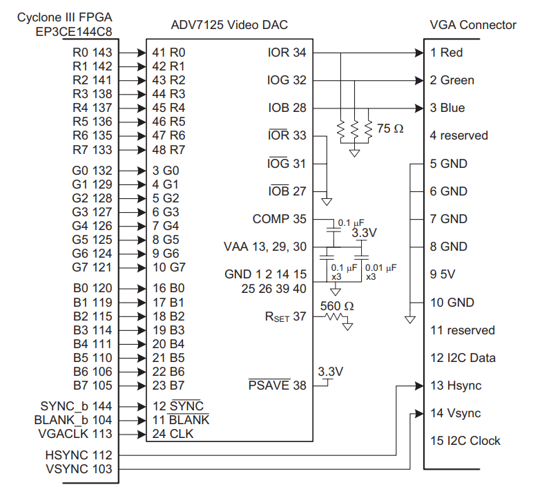
The VGA protocol originated with the intended purpose of displaying images on cathode ray tubes (CRTs) with a resolution of 640 x 480 pixels. These CRTs would strobe an electron beam across the display from left to right and top to bottom, exciting flourescent material to display ultimately display an image. a 15-pin connector was used to transmit the necessary analog color data, vsync/hsync signals, while providing alternative functions with I2C clock and data signals.

While the original specification included additional functionality such as I²C data channels (DDC) for EDID communication, in this project we only use: - 4-bit Color Data (r, g, b): These digital outputs from the FPGA are converted into analog signals using a simple resistor DAC. - Horizontal Sync (hs): A signal controlling the start of a new display line. - Vertical Sync (vs): A signal controlling the start of a new frame (top of the display).
Other signals such as the I2C clock and data were not used.

Scan Line Timing
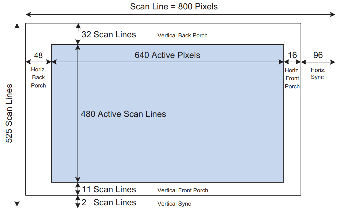
A single scan line in the VGA protocol is divided into several segments:
Front Porch: This is the time between the end of the visible line and the start of the horizontal sync pulse. It allows the electron beam to move from the end of the line back to the start of the next line.
Horizontal Sync Pulse: This is a short pulse that indicates the end of a scan line and the start of the next. It is used to synchronize the display’s horizontal scanning.
Back Porch: This is the time after the horizontal sync pulse and before the start of the visible line. It allows the electron beam to stabilize before starting to draw the next line.
Visible Area: This is the part of the scan line where the actual image data is displayed.
Frame Timing
Similarly, a frame is divided into:
Vertical Front Porch: The time between the end of the visible frame and the start of the vertical sync pulse.
Vertical Sync Pulse: A pulse indicating the end of a frame and the start of the next. It synchronizes the vertical scanning.
Vertical Back Porch: The time after the vertical sync pulse and before the start of the visible frame.
Visible Frame: The area where the image data is displayed.
These timing segments are crucial for ensuring that the display correctly interprets the signals and displays the image as intended. In order to write the FPGA code we made reference of Chapter 9 in the book Digital Design and Computer Architecture by David Harris and Sarah Harris. We will describe the FPGA design in the next section.
VGA Block Diagram
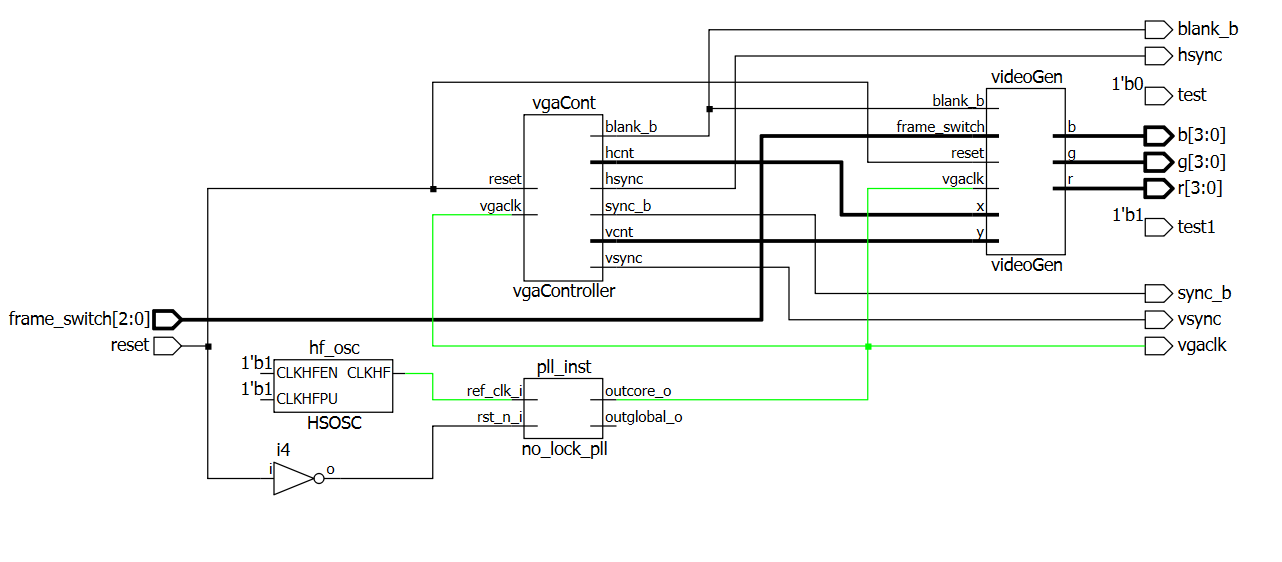
The VGA module is responsible for generating the necessary signals to drive a VGA display. It consists of several key components:
VGA Module: This is the top-level module that integrates all the components required for VGA signal generation. It takes inputs such as a reset signal and a frame switch, and outputs VGA clock, sync signals, and color data.
Internal High-Speed Oscillator (HSOSC): Provides a base clock signal which is used by the PLL to generate the VGA clock.
Phase-Locked Loop (PLL): Converts the internal oscillator’s frequency to the required 25 MHz VGA clock.
VGA Controller: Generates horizontal and vertical sync signals, as well as blanking signals, based on the VGA timing specifications.
Video Generator (videoGen): Determines the color of each pixel based on the current frame and coordinates. It uses a multiplexer to select the appropriate frame data and checks if the current pixel is within any defined rectangles.
Frame Modules: Each frame module (e.g.,
image_frame0,image_frame1, etc.) defines a set of rectangles representing different parts of an image for a specific frame.Frame Multiplexer (frame_mux): Selects the appropriate frame data based on the
frame_switchinput.Rectangle and Line Generators: These modules determine if the current pixel is within a defined rectangle or on a line, respectively.
The block diagram below illustrates the interconnections between these components:

Parallel Communication Interface
To control which frame is displayed, the microcontroller sets 3 I/O lines to a specific pattern of states (0-7 in binary) to select one of eight predefined frames. Each frame corresponds to a particular arrangement of graphical elements. This simple and low-bandwidth interface allows the microcontroller to direct the FPGA’s video frame output without requiring the MCU to handle the stringent timing or memory requirements associated with full video generation.