Hardware
The goal of this hardware is to facilitate communication between the MCU, FPGA, and IMUs. The schematic below provides a comprehensive overview of the system, including all individual components.

MCU/IMU Hardware
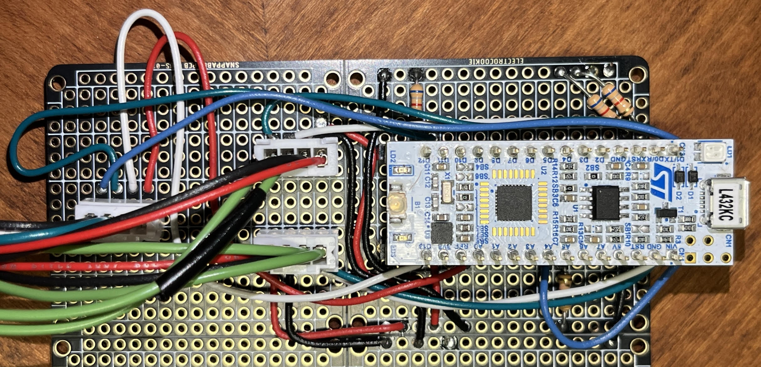
I2C operates simply, requiring only an SCL, SDA, and power and ground lines for each IMU. The key thing to remember with I2C hardware is that the SCL and SDA lines are idle high, so they require 1kΩ to 10kΩ pull-up resistors, as shown in the schematic above with the 6.8kΩ resistors. As described in the software section, the SCL1 and SDA1 lines corresponding to the I2C1 peripheral enable communication with multiple IMUs on a single bus, while the SCL3 and SDA3 lines corresponding to the I2C3 peripheral are connected to only one IMU. Below, you can see an image of the finished hardware implementation in real life. It was soldered onto a protoboard with 4-pin connectors for the I2C peripherals and for the state variables going to the FPGA, making the system more durable and modular.

Below is the complete MCU + (3x) IMUs circuit, including wiring harnesses and Velcro straps. The two IMUs on the right attach to the right leg: the blue IMU (with the address terminal jumped) is positioned at the center right of the shin segment, while the white IMU is strapped to the center right of the femur segment. The left IMU is attached with the cable facing downward at the center of the chest, with the screws on the right side of the user. STEMMA quick-connect cables, spliced onto measured stranded wire extensions, form the wiring harnesses, ensuring easy, reliable, and modular interfacing with the IMUs. The ends of both the leg and torso sections are connected to the MCU protoboard via 4-pin wire-to-board connectors.

FPGA/VGA Hardware
For this project, the Field-Programmable Gate Array (FPGA) was utilized to generate and drive a VGA display signal. Although many microcontrollers can perform VGA output through bit-banging or specialized peripherals, producing a stable, high-resolution image at a standard VGA refresh rate (e.g., 640x480 at 60 Hz) can be computationally expensive and timing-sensitive. Microcontrollers running linear, sequential instructions often struggle to reliably meet these stringent timing requirements without additional support. In contrast, an FPGA can implement dedicated, parallel hardware logic, including a custom pixel pipeline and timing generation circuitry. This approach offloads the computational burden from the microcontroller and ensures that the critical VGA timing parameters (horizontal/vertical sync pulses, front/back porches, and active video periods) are consistently maintained. As a result, the FPGA ensures smooth, flicker-free 60 Hz display updates.
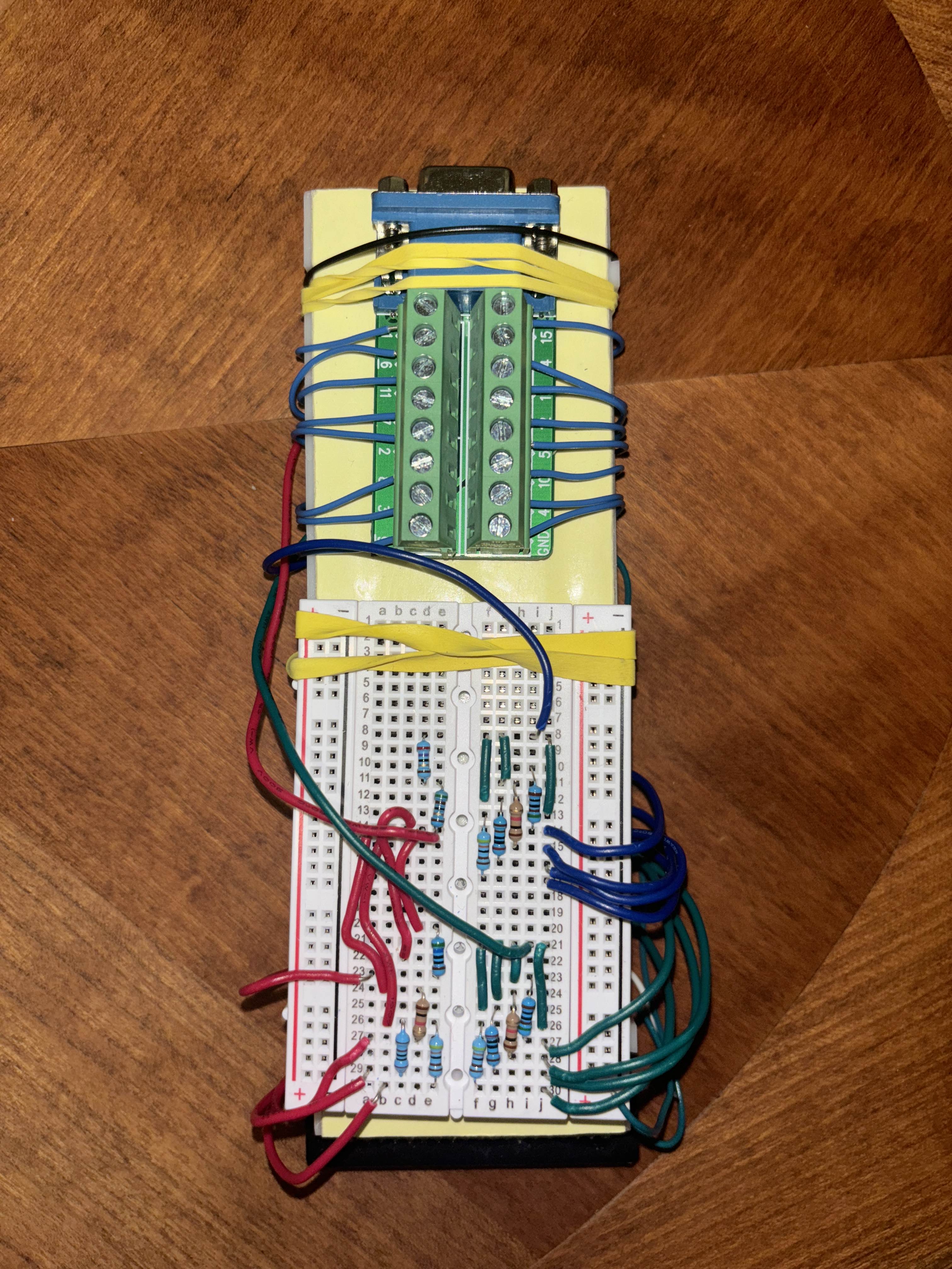
DAC Design
The FPGA outputs digital color information (4 bits per channel: red, green, blue) at a 3.3 V logic level. To meet the VGA standard, these must be translated into analog signals typically ranging from 0 V (black) to about 0.7 V (full brightness). To achieve this, a simple resistor-based DAC is used. By choosing resistor values in a binary-weighted fashion (e.g., 500Ω, 1kΩ, 2kΩ, and 4kΩ for each bit), and by relying on the 75Ω input impedance of the VGA input as part of the output stage, we can generate the correct voltage range.
