Keypad Scanner
Intro & Design Approach
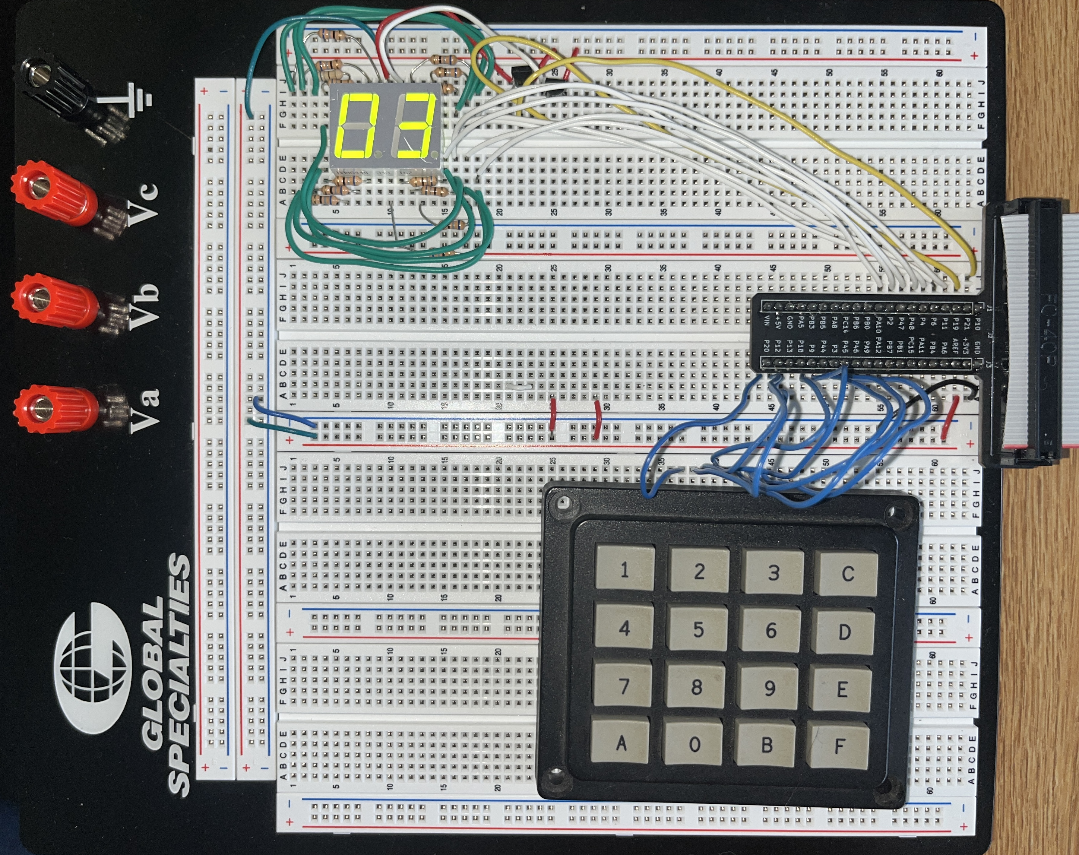
This lab utilized a 4x4 keypad scanner in tandem with a time-multiplexed dual 7-segment display, which was developed during Lab 2. The final goal was to update the right 7-segment display with each button press on the keypad, while the left display would show the previously pressed value. This functionality was implemented using a finite state machine (FSM) and next-state logic to simultaneously scan the keypad rows and decode which button was being pressed. Debouncing logic was also implemented to handle button bounce within the keypad.
Design
This section goes into the hardware and software design specifics
Hardware
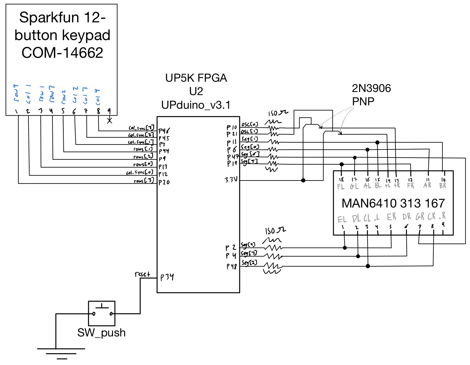
The system hardware consists of two main sections: segment control and keypad input. The segment control section is identical to the design from Lab 2, utilizing two 2N3906 PNP transistors and time-multiplexing logic to display two separate outputs on the dual 7-segment display. The keypad input section accesses the desired row and column pins. When a column is powered and a button is pressed in that column, a button press is registered if the corresponding row pin is active low.
Due to the internal hardware of the keypad, when a column is powered and a key is pressed, the specific row being pressed is unknown, making it difficult to determine the exact button. To resolve this, a row-scanning method is used, which sets one row active low at a time using next state logic described in the FSM section. Since the column pins are active high, if a button is pressed in a column corresponding to an active low row, we can track which row is being scanned and which column pin is pulled down to 0, allowing us to accurately decode the button press.
FSM
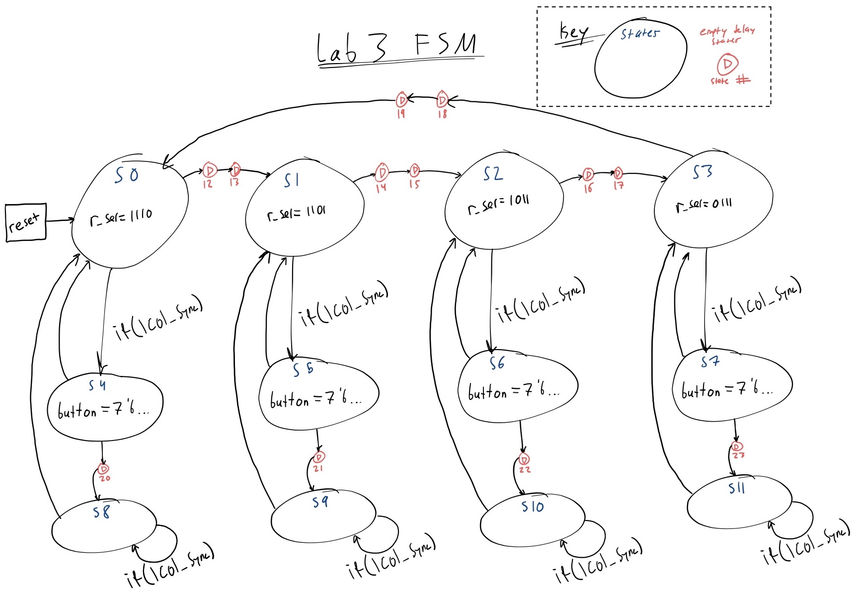
Top Row States (Idle/Row Selection): This state acts as the pathway between all four row scans, determining which row is selected as active low. The FSM cycles through these top states rapidly when no button is pressed. Delay states are used between the top states to ensure button presses are registered in time.
Middle Row States (Button Detection/Decode): Upon detecting a button press, the FSM transitions from the top state to this second state for one clock cycle. Here, the button decoder is engaged, and the corresponding segment display values are updated. A delay state is used between the middle and bottom state to ensure segment values are assigned correctly.
Bottom Row States (Hold/Wait): After the button press is decoded, the FSM moves to the third state, which remains active as long as the button is pressed. No new logic occurs in this state, but it prevents further row scanning while a button is being held. This ensures that when one button is pressed, a second concurrent button press does not update the display.
Block Diagram
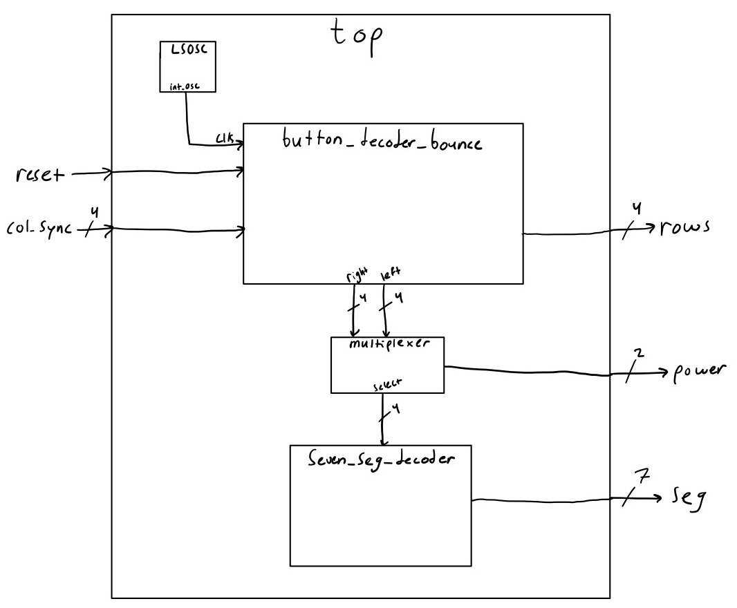
Figure 4 below displays the module communication logic for the System Verilog code that programmed the FPGA. Notibly we have a top, button_decode_bounce, and seven_seg_decoder modules.
top: The overseeing connection module and direct communication with I/O. Also includes the time-multiplexer and Low Speed Oscillator (LSOSC) clk source.
button_decode_bounce: button decoder, debouncer, and row scan generator.
seven_seg_decoder: decodes the button pressed into 7-segment display outputs.
Design Simulation
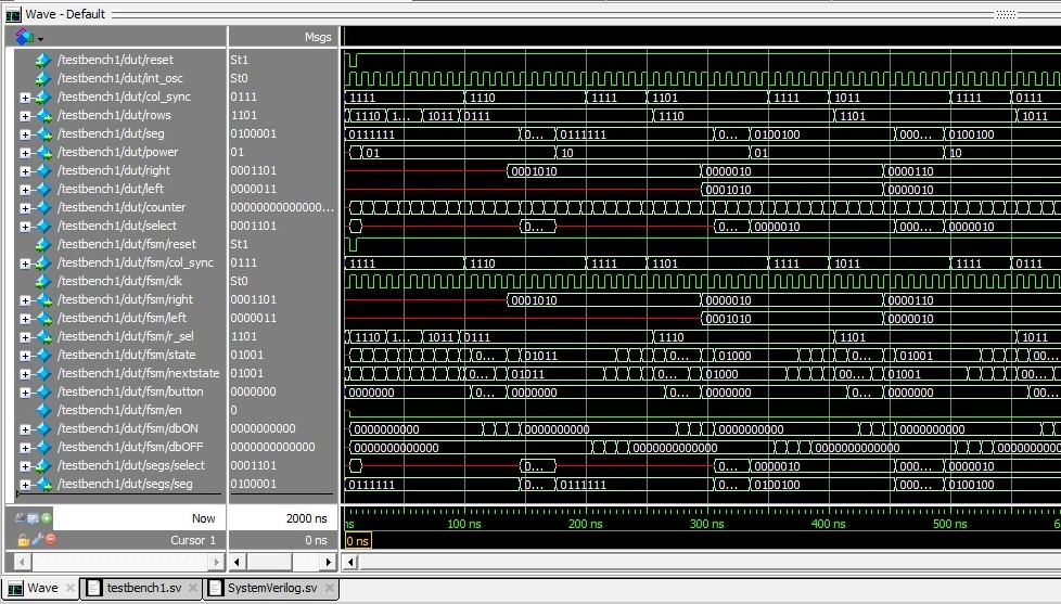
ModelSim simulation software was used to simulate the waveforms of my SystemVerilog code. Figure 5 below shows an example of the waveforms flowing in and out of all included modules.
To ensure proper functionality, I began by analyzing the output, and worked backward through the waveforms if the output was unexpected. The waveform below is an example of a successful simulation, where the correct right and left values are fed into select based on col_sync and power.
Results
This lab resulted in a functioning time-multiplexed dual 7-segment display controlled by a 16-button array using a row scanning strategy. The button debouncing is effective, minimizing any unwanted consecutive inputs due to the button irregularities. This lab took me about 30 hours to complete.
Reflection
I had always heard that this would be a difficult lab, and that was no lie. While I took a long time on this lab, I learned a lot about how to effectively use my time on a technically complex task. This lab served as a vehicle for me to advance my HDL coding skills and simulation debugging. I had a lot of fun; I am glad I had this experience and will go into future projects with more experience in meticulous design, debugging, and time management strategies.