Time-Multiplexed Dual 7-Segment Display
Intro & Design Approach
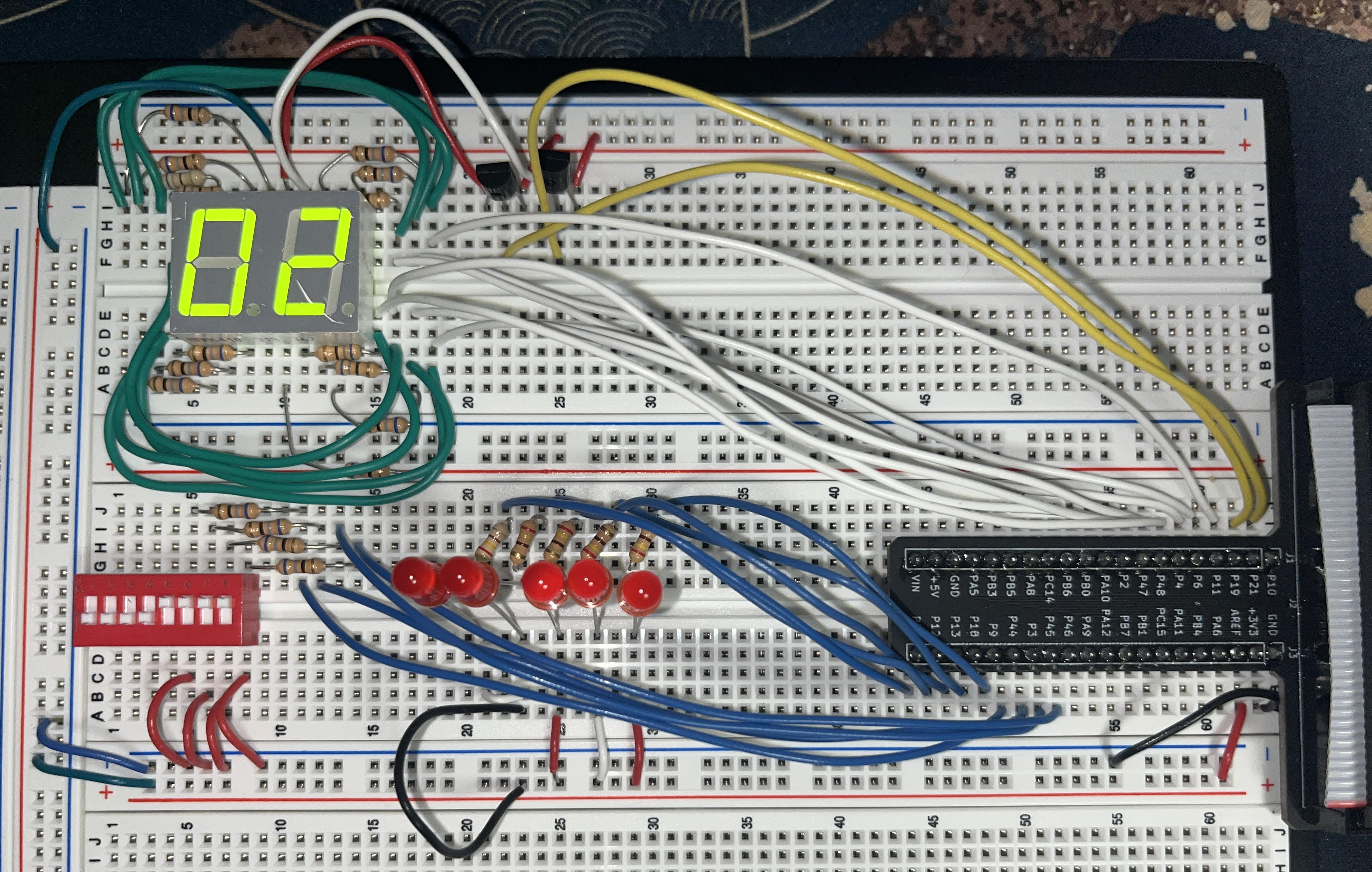
In this lab, a design was implemented on an FPGA to time-multiplex between two 7-segment displays, each showing separate values based on its own 4-bit binary input. Two simple transistor circuits were used to alternate between the respective 7-segment displays. Additionally, the design required the sum of these two 4-bit inputs to be displayed in binary on a 5-bit line of LEDs.

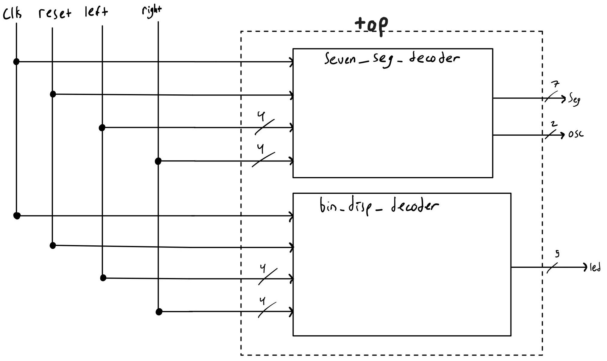
The design process began with a block diagram, where I created a top module and two submodules:
- seven_seg_decoder: decodes inputs to 7-seg pin assignments
- bin_disp_decoder: sums input values and writes that sum in binary to led
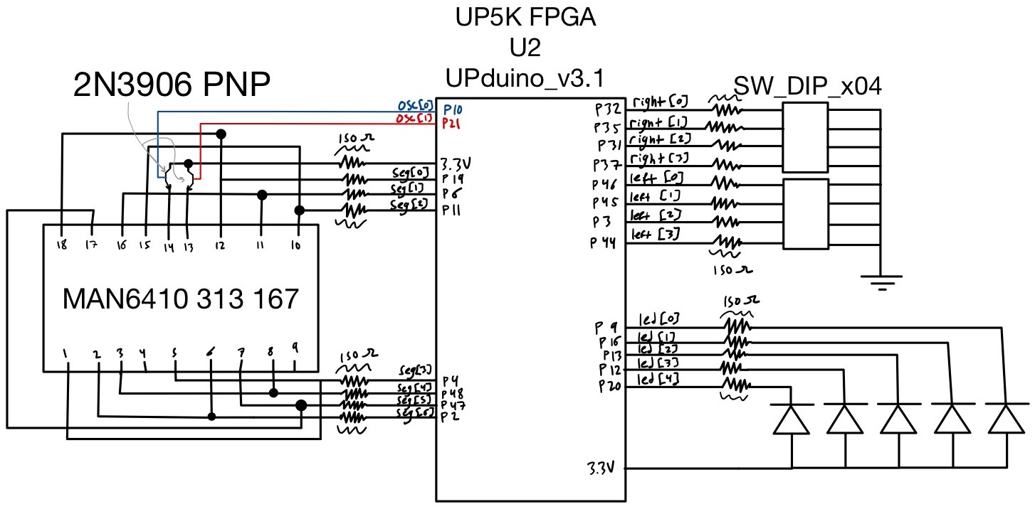
I then created a circuit schematic, which allowed me to visualize physical pin assignments and accurately represent those in my SystemVerilog.
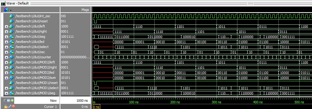
A wavefrom was then used to simulate, debug, and validate system functions.
Block Diagram
In SystemVerilog, when programming the UPduino FPGA, a counter was used in conjunction with the on-board high-speed oscillator (HSOSC) to generate an internal clock signal named int_osc. The int_osc influenced the counter variable, and was then used to time-multiplex between the displays and manage other internal logic. Combinational logic was subsequently implemented to handle the 7-segment display outputs. A simple assign statement was used to generate the LED binary outputs.

Circuit Schematic

Simulation
During the design process, waveform generation was performed to debug and verify the expected functionality. As shown in the figure below, with both right and left inputs, the output seg correctly provides the decoded signal for the corresponding 7-segment display. The osc, which toggles the time multiplexing behavior, captures the output seg for each display, demonstrating that it accurately reflects the expected decoded input values. We can also observe that the 5-bit summation represented as led correctly gets value sum corresponing to right + left correctly. This validates the functionality of the system.

Results & Discussion
This lab resulted in a working time-multiplexed dual 7-segment display that coorectly displays hexidecimal digits 1-F independantly, clearly, and without bleeding. As well as a functioning 5-bit LED display showing the binary combination of the two 4-bit inputs.
The counter variable, incremented by the internal clock signal (int_osc), controls the oscillation speed between two different 7-segment displays using a selector. While this provides adequate control for the current application, developing a more precise counter mechanism could further optimize performance and improve accuracy in future work.
This lab took approximately 13 hours to complete. Significant challenges were encountered early in the implementation stage. Utilizing wave forms and test benched earlier on would have helped and I will do so going forward.